nRESET and POWER-DOWN S3C8245/P8245/C8249/P8249
8-2
HARDWARE nRESET VALUES
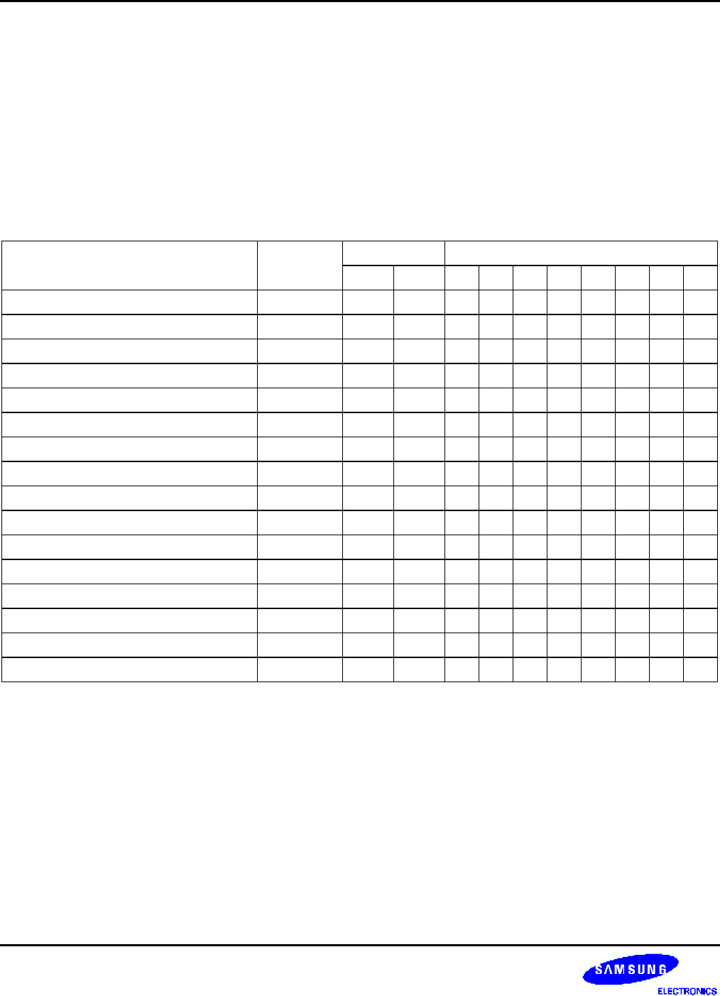
Table 8-1, 8-2, 8-3 list the reset values for CPU and system registers, peripheral control registers, and peripheral
data registers following a reset operation. The following notation is used to represent reset values:
— A "1" or a "0" shows the reset bit value as logic one or logic zero, respectively.
— An "x" means that the bit value is undefined after a reset.
— A dash ("–") means that the bit is either not used or not mapped, but read 0 is the bit value.
Table 8-1. S3C8245/C8249 Set 1 Register and Values after nRESET
Register Name Mnemonic Address Bit Values after nRESET
Dec Hex 7 6 5 4 3 2 1 0
LCD Control Register LCON 208 D0H 0 0 0 0 0 0 0 0
LCD Mode Register LMOD 209 D1H 0 0 0 0 0 0 0 0
Interrupt Pending Register INTPND 210 D2H – – – – – 0 0 0
Basic Timer Control Register BTCON 211 D3H 0 0 0 0 0 0 0 0
Clock Control Register CLKCON 212 D4H 0 0 0 0 0 0 0 0
System Flags Register FLAGS 213 D5H x x x x x x 0 0
Register Pointer (High Byte) RP0 214 D6H 1 1 0 0 0 – – –
Register Pointer (Low Byte) RP1 215 D7H 1 1 0 0 1 – – –
Stack Pointer (High Byte) SPH 216 D8H x x x x x x x x
Stack Pointer (Low Byte) SPL 217 D9H x x x x x x x x
Instruction Pointer (High Byte) IPH 218 DAH x x x x x x x x
Instruction Pointer (Low Byte) IPL 219 DBH x x x x x x x x
Interrupt Request Register IRQ 220 DCH 0 0 0 0 0 0 0 0
Interrupt Mask Register IMR 221 DDH x x x x x x x x
System Mode Register SYM 222 DEH 0 – – x x x 0 0
Register Page Pointer PP 223 DFH 0 0 0 0 0 0 0 0


