


Troubleshooting
26
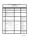
Table 3-6. A10 Auxiliary Power Supply Troubleshooting
Procedure Action
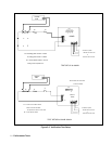
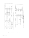
See figures 6-7 and 6-8 for test points and schematic.
Control Circuits 1. Apply 20 Vdc between TP7(+) and TP1(-).
2. Verify waveform at TP2 to TP1. 0 V to >15 V at approximately 60 kHz, duty cycle
40% to 50%.
3. Check drive to Ql and Q4 . Connect scope common to CR13 anode, verify waveform
at gate drive resistors R10 and R28 is swinging between +12Vpk and –12Vpk at
approximately 60 kHz, duty cycle 40 to 50%.
Outputs 1. Apply 20 Vdc between TP7(+) and TP1(-). Add a 10 ohm 25 W resistor across R13.
2. Apply 300 Vdc between Jl-1,2 (+) to Jl-5,6 (-).
3. Verify the 15 SW1 voltage across R13 is between 14.5 and 15.5 Vdc.
4. Verify the +5 GPIB voltage across R18 is between 4.8 and 5.2 Vdc.
5. Verify the +5V SEC voltage across R33 is between 4.2 and 5.2 Vdc.
6. Verify the fan voltage from J3-1 (+) to J3-5 (-) is between 14.6 and 15.8 Vdc.
Short J4-6 to J3-5 fan voltage should now be between 17.4 and 18.9 Vdc.
7. Verify the +15 analog supply across R43 is between 14.3 and 15.5 Vdc.
8. Verify the –15 analog supply across R48 is between 14.3 and 15.5 Vdc.
*A lower input voltage ( <300 Vdc ) can be used but the expected output voltages must
be recalculated.
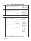
Table 3-7. A14 Option 400 Bias Power Supply Troubleshooting
Procedure Action
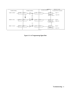
See figure 6-9 and 6-10 for test points and schematic.
Outputs 1. Apply 342 V 50/60 Hz between J2-1 and J2-4.
2. From TP1 (Lo) (Jl-7 ) to Jl-8 measure 26 Vdc +/- 2V.
3. From TP1 (Lo) (Jl-7 ) to Jl-6 measure 26 Vdc +/- 2V.
4. From TP2 (Lo) (Jl -3 ) to Jl -4 measure 19.3 Vdc +/- 2V.
5. From TP2 (Lo) (Jl-3 ) to Jl-2 measure -19.3 Vdc +/- 2V.
6. From TP3 (Lo) (J I -11 ) to J1 -1 0 measure 26 Vdc +/- 2V.
7. From TP2 (Lo) (Jl-3 ) to Jl-12 measure -26 Vdc +/- 2V.
*A lower input voltage ( <342 Vac ) can be used, but the expected output voltages must
be recalculated.