


21
State analysis calibration procedure
This process is in large part the same for both use in the 7 card Read and Write
configuration at 800MT/s and for the 4 card configurations. Differences are noted.
1) Start a memory test program that creates a good mixture of reads and writes in a
single TimingZoom trace. A trigger on a write may be required if the test program does
not have a mix or reads and writes in close proximity.
Note that in addition to looking for the DDR commands the #S0:1 and CKE0:1 signals are
used to determine if the command is actually addressing a memory chip. The Write –
Command:CK2_TZ signal is used to make sure the command is sampled on the rising edge
of the DIMM clock (since that is when the DDR command bus is valid).
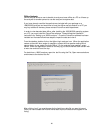
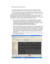
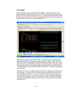
2) Bring up a waveform display and add the TimingZoom labels for the command
clock, chip selects, and DQS0 (Write – Command:CK2_TZ, #S0_TZ, DQS8-
0_TZ[0]) and the data bus labels for Writes (Data63-32_R/Fand Data31-0_R/F) in
the waveform view. Scroll the waveforms to find the start of a Write burst. You will
see this by finding where the DQS0 strobe becomes active.
Note: The 4 card configurations have only 2 sets of Data labels.
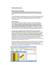
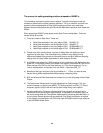
3) Now the time delay from the closest rising edge of Write – Command:CK2_TZ prior
to the center of the write data eyes can be measured. This will be the DATA_rising
point. Place a marker on that edge of the Write – Command:CK2_TZ. Place the
other marker in the center of the data valid region for the data label. You may find it
easier to identify this point by locating the point on one of the DQS signals that is
equal distances from the edges. Note the 103 ps delay between the markers as
shown below.
The 4 card config for 667MT/s will use delays measured from the nearest rising of
falling edge of the state clock.