Endpoint Block Plus v1.8 for PCI Express www.xilinx.com 19
UG343 June 27, 2008
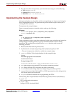
Implementing the Example Design
R
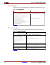
2. Run the script that corresponds to your simulation tool using one of the following:
• VCS:
simulate_vcs.sh
• Cadence IUS: simulate_ncsim.sh
• ModelSim: vsim -do simulate_mti.do
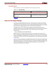
Implementing the Example Design
After generating the core, the netlists and the example design can be processed using the
Xilinx implementation tools. The generated output files include scripts to assist you in
running the Xilinx software.
To implement the example design:
Open a command prompt or terminal window and type the following:
Windows
ms-dos> cd <project_dir>\<component_name>\implement
ms-dos> implement.bat
Linux
% cd <project_dir>/<component_name>/implement
% ./implement.sh
These commands execute a script that synthesizes, builds, maps, and place-and-routes the
example design, and then generates a post-par simulation model for use in timing
simulation. The resulting files are placed in the
results directory and execute the
following processes:
1. Removes data files from the previous runs.
2. Synthesizes the example design using either Synplicity Synplify or XST.
- The core is instanced as a black box within the example design.
3.
ngdbuild. Builds a Xilinx design database for the example design.
Inputs:
Part-Package-Speed Grade selection:
XC5VLX50T-FF1136-1
Example design UCF:
xilinx_pci_exp_blk_plus_1_lane_ep-XC5VLX50T-FF1136-1.ucf
4. map: Maps design to the selected FPGA using the constraints provided.
5.
par: Places cells onto FPGA resources and routes connectivity.
6. trce: Performs static timing analysis on design using constraints specified.
7.
netgen: Generates a logical Verilog HDL or VHDL representation of the design and an
SDF file for post-layout verification.
8.
bitgen: Generates a bitstream file for programming the FPGA.
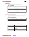
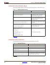
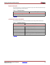
The following FPGA implementation related files are generated in the results directory:
•
routed.bit
FPGA configuration information.
• routed.v[hd]
Verilog or VHDL functional Model.


