8XC251SA, SB, SP, SQ USER’S MANUAL
4-4
4.3 THE CONFIGURATION BITS
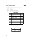
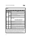
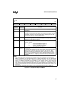
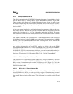
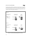
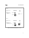
This section provides a brief description of the configuration bits contained in the configuration
bytes (Figures 4-3 and 4-4). UCONFIG0 and UCONFIG1 have five wait state bits: WSA1:0#,
WSB1:0#, and WSB.
• UCON. Configuration byte location selector.
• SRC. Selects source mode or binary mode opcode configuration.
• INTR. Selects the bytes pushed onto the stack by interrupts.
• EMAP#. Maps on-chip code memory (16-Kbyte devices only) to memory region 00:.
The following bits configure the external memory interface.
• PAGE#. Selects page/nonpage mode and specifies the data port.
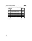
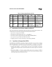
• RD1:0. Selects the number of external address bus pins and the address range for RD#, WR,
and PSEN#. See Table 4-2.
• XALE#. Extends the ALE pulse.
• WSA1:0#. Selects 0, 1, 2, or 3 pre-programmed wait states for all regions except 01:.
• WSB1:0#. Selects 0 - 3 pre-programmed wait states for memory region 01:.
• EMAP#. Affects the external memory interface in that, when asserted, addresses in the
range 00:E000H–00:FFFH access on-chip memory.
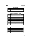
Table 4-1. External Addresses for Configuration Array
Size of External
Address Bus
(Bits)
Address of
Configuration Array on
External Bus (2)
Address of
Configuration Bytes
on External Bus (1)
16 FFF8H–FFFFH UCONFIG1: FFF9H
UCONFIG0: FFF8H
17 1FFF8H–1FFFFH UCONFIG1: 1FFF9H
UCONFIG0: 1FFF8H
18 3FFF8H–3FFFFH UCONFIG1: 3FFF9H
UCONFIG0: 3FFF8H
NOTES:
1. When EA# = 0, the reset routine retrieves UCONFIG0 and UCONFIG1 from
external memory using internal addresses FF:FFF8H and FF:FFF9H, which
appear on the microcontroller external address bus (A17, A16, A15:0).
2. The upper six bytes of the configuration array are reserved for future use.


