8XC251SA, SB, SP, SQ USER’S MANUAL
9-2
9.1.1 Alternate Port Usage
PCA modules 3 and 4 share port pins with the real-time wait state and address functions as fol-
lows:
• PCA module 3 — P1.6/CEX3/WAIT#
• PCA module 4 — P1.7/CEX4/A17/WCLK
When the real-time wait state functions are enabled (using the WCON register), the correspond-
ing PCA modules are automatically disabled. Configuring the 8XC251Sx to use address line A17
(specified by UCONFIG0, bits RD1:0) overrides the PCA module 3 and WCLK functions. When
a real-time wait state function is enabled, do not use the corresponding PCA module.
NOTE
It is not advisable to alternate between PCA operations and real-time wait state
operations at port 1.6 (CEX3/WAIT#) or port 1.7 (CEX4/WCLK). See section
13.5, “External Bus Cycles with Real-time Wait States.”
9.2 PCA TIMER/COUNTER
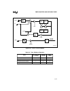
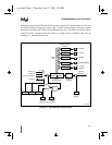
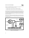
Figure 9-1 depicts the basic logic of the timer/counter portion of the PCA. The CH/CL special
function register pair operates as a 16-bit timer/counter. The selected input increments the CL
(low byte) register. When CL overflows, the CH (high byte) register increments after two oscil-
lator periods; when CH overflows it sets the PCA overflow flag (CF in the CCON register) gen-
erating a PCA interrupt request if the ECF bit in the CMOD register is set.
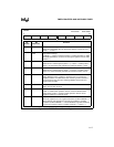
The CPS1 and CPS0 bits in the CMOD register select one of four signals as the input to the
timer/counter (Figure 9-7).
• F
OSC
/12. Provides a clock pulse at S5P2 of every peripheral cycle. With F
OSC
= 16 MHz, the
time/counter increments every 750 nanoseconds.
• F
OSC
/4. Provides clock pulses at S1P2, S3P2, and S5P2 of every peripheral cycle. With
F
OSC
= 16 MHz, the time/counter increments every 250 nanoseconds.
• Timer 0 overflow. The CL register is incremented at S5P2 of the peripheral cycle when
timer 0 overflows. This selection provides the PCA with a programmable frequency input.
• External signal on P1.2/ECI. The CPU samples the ECI pin at S1P2, S3P2, and S5P2 of
every peripheral cycle. The first clock pulse (S1P2, S3P2, or S5P2) that occurs following a
high-to-low transition at the ECI pin increments the CL register. The maximum input
frequency for this input selection is F
OSC
/8.
For a description of peripheral cycle timing, see section 2.2.2, “Clock and Reset Unit.”


