13-11
EXTERNAL MEMORY INTERFACE
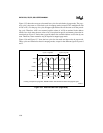
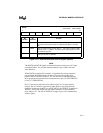
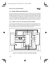
Figure 13-11. Real-time Wait State Control Register (WCON)
NOTE
The WAIT# and WCLK signals are alternate functions for the port 1.6:7 input
and output buffers. Use of other alternate functions may conflict with wait
state operation.
When WAIT# is enabled, PCA module 3 is disabled and resumes operation
only when the WAIT# function is disabled. The same relationship exists
between WCLK and PCA module 4. It is not advisable to alternate between
PCA operations and real-time wait-state operations at port 1.6 (CEX3/WAIT#)
or port 1.7 (CEX4/WCLK).
Port 1.7 can also be enabled to drive address signal A17 in some memory
designs. The A17 address signal always takes priority over other alternate
functions (in this case, both PCA.4 and WCLK). Even if RTWCE is enabled in
WCON.1, the WCLK output does not appear during bus cycles enabled to
drive address A17. The use of WAIT# as an input on port 1.6 is unaffected by
address signals.
WCON
Address: S:A7H
Reset State: XXXX XX00B
7 0
— — — — — — RTWCE RTWE
Bit
Number
Bit
Mnemonic
Function
7:2 — Reserved:
The values read from these bits are indeterminate. Write “0” to these
bits.
1 RTWCE Real-time WAIT CLOCK enable. Write a ‘1’ to this bit to enable the WAIT
CLOCK on port 1.7 (WCLK). The square wave output signal is one-half
the oscillator frequency.
0 RTWE Real-time WAIT# enable. Write a ‘1’ to this bit to enable real-time wait-
state input on port 1.6 (WAIT#).


