8XC251SA, SB, SP, SQ USER’S MANUAL
C-18
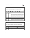
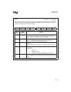
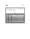
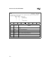
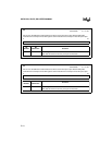
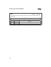
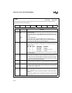
P2
Address: S:A0H
Reset State: 1111 1111B
Port 2. P2 is the SFR that contains data to be driven out from the port 2 pins. Read-modify-write
instructions that read port 2 read this register. Other instructions that read port 2 read the port 2 pins.
7 0
P2 Contents
Bit
Number
Bit
Mnemonic
Function
7:0 P2.7:0 Port 2 Register:
Write data to be driven onto the port 2 pins to these bits.
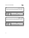
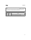
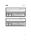
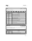
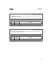
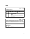
P3
Address: S:B0H
Reset State: 1111 1111B
Port 3. P3 is the SFR that contains data to be driven out from the port 3 pins. Read-modify-write
instructions that read port 3 read this register. Other instructions that read port 3 read the port 3 pins.
7 0
P3 Contents
Bit
Number
Bit
Mnemonic
Function
7:0 P3.7:0 Port 3 Register:
Write data to be driven onto the port 3 pins to these bits.


