11-3
MINIMUM HARDWARE SETUP
11.3 CLOCK SOURCES
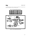
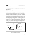
The 8XC251Sx can obtain the system clock signal from an external clock source (Figure 11-3) or
it can generate the clock signal using the on-chip oscillator amplifier and external capacitors and
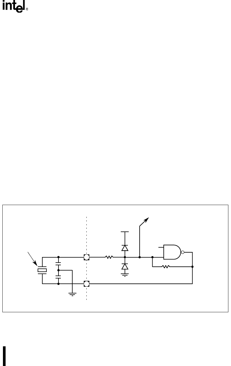
resonator (Figure 11-2).
11.3.1 On-chip Oscillator (Crystal)
This clock source uses an external quartz crystal connected from XTAL1 to XTAL2 as the fre-
quency-determining element (Figure 11-2). The crystal operates in its fundamental mode as an
inductive reactance in parallel resonance with capacitance external to the crystal. Oscillator de-
sign considerations include crystal specifications, operating temperature range, and parasitic
board capacitance. Consult the crystal manufacturer’s data sheet for parameter values. With high
quality components, C1 = C2 = 30 pF is adequate for this application.
Pins XTAL1 and XTAL2 are protected by on-chip electrostatic discharge (ESD) devices, D1 and
D2, which are diodes parasitic to the R
F
FETs. They serve as clamps to V
CC
and V
SS
. Feedback
resistor R
F
in the inverter circuit, formed from paralleled n- and p- channel FETs, permits the PD
bit in the PCON register (Figure 12-1 on page 12-2) to disable the clock during powerdown.
Noise spikes at XTAL1 and XTAL2 can disrupt microcontroller timing. To minimize coupling
between other digital circuits and the oscillator, locate the crystal and the capacitors near the chip
and connect to XTAL1, XTAL2, and V
SS
with short, direct traces. To further reduce the effects of
noise, place guard rings around the oscillator circuitry and ground the metal crystal case.
Figure 11-2. CHMOS On-chip Oscillator
A4143-02
XTAL2
XTAL1
C1
C2
V
CC
PD#
To Internal
Timing Circuit
8XC251S
x
R
F
Quartz Crystal
or Ceramic Resonator
D1
D2


