7-1
CHAPTER 7
INPUT/OUTPUT PORTS
7.1 INPUT/OUTPUT PORT OVERVIEW
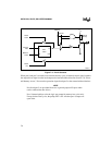
The 8XC251Sx uses input/output (I/O) ports to exchange data with external devices. In addition
to performing general-purpose I/O, some ports are capable of external memory operations (see
Chapter 13, “External Memory Interface”); others allow for alternate functions. All four
8XC251Sx I/O ports are bidirectional. Each port contains a latch, an output driver, and an input
buffer. Port 0 and port 2 output drivers and input buffers facilitate external memory operations.
Port 0 drives the lower address byte onto the parallel address bus, and port 2 drives the upper ad-
dress byte onto the bus. In nonpage mode, the data is multiplexed with the lower address byte on
port 0. In page mode, the data is multiplexed with the upper address byte on port 2. All port 1 and
port 3 pins serve for both general-purpose I/O and alternate functions (see Table 7-1).
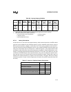
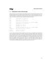
Table 7-1. Input/Output Port Pin Descriptions
Pin
Name
Type
Alternate
Pin Name
Alternate Description
Alternate
Type
P0.7:0 I/O AD7:0 Address/Data (Nonpage Mode), Address (Page Mode) I/O
P1.0 I/O T2 Timer 2 Clock Input/Output I/O
P1.1 I/O T2EX Timer 2 External Input I
P1.2 I/O ECI PCA External Clock Input I
P1.3 I/O CEX0 PCA Module 0 I/O I/O
P1.4 I/O CEX1 PCA Module 1 I/O I/O
P1.5 I/O CEX2 PCA Module 2 I/O I/O
P1.6 I/O CEX3/WAIT# PCA Module 3 I/O I/O
P1.7 I/O CEX4/A17/WCLK PCA Module 4 I/O or 18th Address Bit I/O(O)
P2.7:0 I/O A15:8 Address (Nonpage Mode), Address/Data (Page Mode) I/O
P3.0 I/O RXD Serial Port Receive Data Input I (I/O)
P3.1 I/O TXD Serial Port Transmit Data Output O (O)
P3.2 I/O INT0# External Interrupt 0 I
P3.3 I/O INT1# External Interrupt 1 I
P3.4 I/O T0 Timer 0 Input I
P3.5 I/O T1 Timer 1 Input I
P3.6 I/O WR# Write Signal to External Memory O
P3.7 I/O RD#/A16 Read Signal to External Memory or 17th Address Bit O


