


Instruction Manual
748213-S
April 2002
Rosemount Analytical Inc. A Division of Emerson Process Management Circuit Analysis 5-1
Model 755R
SECTION 5
CIRCUIT ANALYSIS
5-1 CIRCUIT OPERATION
The electronic circuitry of the Model 755R
Oxygen Analyzer consists of the following:
•
A detector compartment heater circuit.
•
A detector heater circuit.
•
A ±15 VDC power supply.
•
A voltage regulating circuit for a stable
light source.
•
A detector circuit with a first-stage am-
plifier to provide a feedback current for
mechanical feedback to the detector
and a scaling amplifier circuit to give an
output change of 0 to +2.5 V for a 0 to
100% change of the operating span.
•
A digital output circuit for the digital
read-out.
•
An analog output circuit for recorder,
optional alarms and current output.
5-2
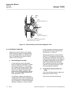
±15 VDC POWER SUPPLY
Refer to Drawing 617186. The components
of the ±VDC power supply circuit are located
in the lower left-hand corner of the Power
Supply Board. 19 VAC should be measured
with respect to ground at CR5 (WO4). +15
VDC should be measured at the C27 (+)
lead and -15 VDC at the C28 (-) lead. If the
specified voltage measurements are ob-
tained, the power supply is working cor-
rectly.
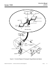
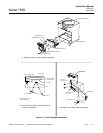
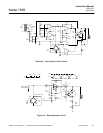
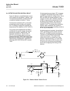
5-3 CASE HEATER CONTROL CIRCUIT
The case heater control circuit utilizes four
voltage-comparators (LM339 quad com-
parator). An understanding of how one of
these comparators functions is necessary
before any circuit analysis can be attempted.
In Figure 5-1 (page 5-2), comparators 1 and
2 are depicted having a comparator within
an overall comparator symbol. Also within
this symbol, the base of the NPN transistor
is connected to the output of the compara-
tor. A -15 VDC is supplied to the emitter.
The collector is illustrated as the overall out-
put for the comparator package.
When the non-inverting terminal of com-
parator 2 is more positive than the inverting
terminal, the transistor does not conduct and
the collector of the transistor or comparator
output is at whatever potential is then pres-
ent on the collector.
When the non-inverting terminal of com-
parator 2 is less positive (more negative)
than the inverting terminal, the transistor
conducts and the output of the comparator is
-15 V. This value is the output of the OR cir-
cuit.
Comparator 2 is biased at 0 volts on the in-
verting terminal. Comparator 1 is biased at
about 159 mV on the non-inverting terminal.
Positive feedback or hysteresis is built into
each comparator circuit for stability or posi-
tive action. This is achieved by the 20 M re-
sistances, R70 and R73.
An approximate 8 V peak-to-peak AC signal
is applied to comparators 1 and 2. As the
signal starts going positive, comparator 2
transistor ceases conducting and compara-
tor 1 transistor is off.
When the signal exceeds the +159 mV on
the non-inverting terminal, it turns on com-
parator 1 and the output is -15 V. Com-
parator 1 stays on until the signal drops
below +159 mV, at which time the output will
be the value of the OR bus.
As the AC signal goes negative with respect
to ground, the transistor of comparator 2
conducts and the output is again -15 V. The