5-9
PROGRAMMING
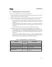
The MCS 251 architecture provides the MUL (multiply) and DIV (divide) instructions for un-
signed 8-bit and 16-bit data (Table A-22 on page A-16). Signed multiply and divide are left for
the user to manage through a conversion process. The following operations are implemented:
• eight-bit multiplication: 8 bits × 8 bits → 16 bits
• sixteen-bit multiplication: 16 bits × 16 bits → 32 bits
• eight-bit division: 8 bits
÷
8 bits → 16 bits (8-bit quotient, 8-bit remainder)
• sixteen-bit division: 16 bits ÷ 16 bits → 32 bits (16-bit quotient, 16-bit remainder)
These instructions operate on pairs of byte registers (Rmd,Rms), word registers (WRjd,WRjs), or
the accumulator and B register (A,B). For 8-bit register multiplies, the result is stored in the word
register that contains the first operand register. For example, the product from an instruction
MUL R3,R8 is stored in WR2. Similarly, for 16-bit multiplies, the result is stored in the dword
register that contains the first operand register. For example, the product from the instruction
MULWR6,WR18 is stored in DR4.
For 8-bit divides, the operands are byte registers. The result is stored in the word register that con-
tains the first operand register. The quotient is stored in the lower byte, and the remainder is stored
in the higher byte. A 16-bit divide is similar. The first operand is a word register, and the result is
stored in the double word register that contains that word register. If the second operand (the di-
visor) is zero, the overflow flag (OV) is set and the other bits in PSW and PSW1 are meaningless.
5.3.3 Logical Instructions
The MCS 251 architecture provides a set of instructions that perform logical operations. The
ANL, ORL, and XRL (logical AND, logical OR, and logical exclusive OR) instructions operate
on bytes and words that are accessed via several addressing modes (Table A-23 on page A-17).
A byte register, word register, or the accumulator can be logically combined with a register, im-
mediate data, or data that is addressed directly or indirectly. These instructions affect the Z and N
flags.
In addition to the CLR (clear), CPL (complement), SWAP (swap), and four rotate instructions that
operate on the accumulator, MCS 251 microcontrollers have three shift commands for byte and
word registers:
• SLL (Shift Left Logical) shifts the register one bit left and replaces the LSB with 0
• SRL (Shift Right Logical) shifts the register one bit right and replaces the MSB with 0
• SRA (Shift Right Arithmetic) shifts the register one bit right; the MSB is unchanged


