8XC251SA, SB, SP, SQ USER’S MANUAL
3-8
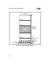
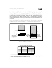
Locations FF:FFF8H–FF:FFFFH are reserved for the configuration array (see Chapter 4, “Device
Configuration”). The two configuration bytes for the 8XC251Sx are accessed at locations
FF:FFF8H and FF:FFF9H; locations FF:FFFAH–FF:FFFFH are reserved for configuration bytes
in future products. Do not attempt to execute code from locations FF:FFF8H–FF:FFFFH. Also,
see the caution on page 4-2 regarding execution of code from locations immediately below the
configuration array.
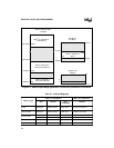
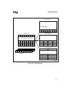
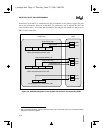
Figure 3-4 also indicates the addressing modes that can be used to access different areas of mem-
ory. The first 64 Kbytes can be directly addressed. The first 96 bytes of general-purpose RAM
(00:0020H–00:007FH) are bit addressable. Chapter 5, “Programming,” discusses addressing
modes.
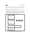
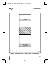
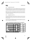
Figure 3-5 on page 3-7 shows how areas of the memory space are implemented by on-chip RAM,
on-chip ROM/OTPROM/EPROM, and external memory. The first 32 bytes of on-chip RAM
store banks 0–3 of the register file (see “8XC251SA, SB, SP, SQ Register File” on page 3-10).
3.2.1 On-chip General-purpose Data RAM
On-chip RAM (512 bytes or 1 Kbyte) is provided for general data storage (Figure 3-5). Instruc-
tions cannot execute from on-chip data RAM. The data is accessible by direct, indirect, and dis-
placement addressing. Locations 00:0020H–00:007FH are also bit addressable.
3.2.2 On-chip Code Memory (83C251SA, SB, SP, SQ/87C251SA, SB, SP, SQ)
The 8XC251Sx is available with 8 Kbytes or 16 Kbytes of on-chip ROM (83C251Sx) or
OTPROM/EPROM (87C251Sx) as well as without on-chip code memory (Figure 3-5). Table 2-1
on page 2-3 lists the amount of on-chip code memory for each device. The on-chip
ROM/OTPROM/EPROM is intended primarily for code storage, although its contents can also
be read as data with the indirect and displacement addressing modes. Following a chip reset, pro-
gram execution begins at FF:0000H. Chapter 14, “Programming and Verifying Nonvolatile
Memory,” describes programming and verification of the ROM/OTPROM/EPROM.
A code fetch within the address range of the on-chip ROM/OTPROM/EPROM accesses the on-
chip ROM/OTPROM/EPROM only if EA# = 1. For EA# = 0, a code fetch in this address range
accesses external memory. The value of EA# is latched when the chip leaves the reset state. Code
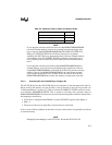
is fetched faster from on-chip code memory than from external memory. Table 3-2 lists the min-
imum times to fetch two bytes of code from on-chip memory and external memory.


