5-7
PROGRAMMING
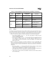
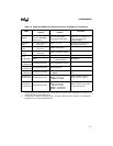
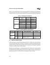
Table 5-4. Addressing Modes for Data Instructions in the MCS
®
251 Architecture
Mode
Address Range of
Operand
Assembly Language
Notation
Comments
Register
00:0000H
–00:001FH
(R0–R7, WR0–WR3,
DR0, DR2) (1)
R0
–R15, WR0–WR30,
DR0
–DR28, DR56, DR60
R0
–R7, WR0–WR6, DR0, and
DR2 are in the register bank
currently selected by the
PSW and PSW1.
Immediate,
2 bits
N.A. (Operand is in the
instruction)
#short = 1, 2, or 4
Used only in increment and
decrement instructions.
Immediate,
8 bits
N.A. (Operand is in the
instruction)
#data8 = #00H–#FFH
Immediate,
16 bits
N.A. (Operand is in the
instruction)
#data16 = #0000H
–#FFFFH
Direct,
8 address bits
00:0000H–00:007FH dir8 = 00:0000H–00:007FH On-chip RAM
SFRs
dir8 = S:080H
–S:1FFH (2)
or SFR mnemonic
SFR address
Direct,
16 address bits
00:0000H–00:FFFFH dir16 = 00:0000H–00:FFFFH
Indirect,
16 address bits
00:0000H–00:FFFFH @WR0–@WR30
Indirect,
24 address bits
00:0000H–FF:FFFFH
@DR0–@DR30, @DR56,
@DR60
Upper 8 bits of DRk must be
00H.
Displacement,
16 address bits
00:0000H–00:FFFFH
@WRj + dis16 =
@WR0 + 0H through
@WR30 + FFFFH
Offset is signed; address
wraps around in region 00:.
Displacement,
24 address bits
00:0000H
–FF:FFFFH
@DRk + dis24 =
@DR0 + 0H through
@DR28 + FFFFH,
@DR56 + (0H–FFFFH),
@DR60 + (0H–FFFFH)
Offset is signed, upper 8 bits
of DRk must be 00H.
NOTES:
1. These registers are accessible in the memory space as well as in the register file (see section 3.3,
“8XC251SA, SB, SP, SQ Register File.”
2. The MCS 251 architecture supports SFRs in locations S:000H–S:1FFH; however, in the 8XC251S
x
,
all SFRs are in the range S:080H–S:0FFH.


