B-7
SIGNAL DESCRIPTIONS
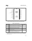
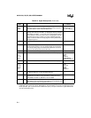
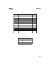
Table B-3. Memory Signal Selections (RD1:0)
RD1:0
P1.7/CEX/
A17/WCLK
P3.7/RD#/A16/ PSEN# WR# Features
0 0 A17 A16 Asserted for
all addresses
Asserted for writes to
all memory locations
256-Kbyte external
memory
0 1 P1.7/CEX4/
WCLK
A16 Asserted for
all addresses
Asserted for writes to
all memory locations
128-Kbyte external
memory
1 0 P1.7/CEX4/
WCLK
P3.7 only Asserted for
all addresses
Asserted for writes to
all memory locations
64-Kbyte external
memory. One
additional port pin.
1 1 P1.7/CEX4/
WCLK
RD# asserted
for addresses
≤ 7F:FFFFH
Asserted for
≥ 80:0000H
Asserted only for
writes to MCS
®
51
microcontroller data
memory locations.
64-Kbyte external
memory. Compatible
with MCS 51 micro-
controllers.
NOTE: RD1:0 are bits 3:2 of configuration byte UCONFIG0 (See Figure 4-3 on page 4-6).


