8XC251SA, SB, SP, SQ USER’S MANUAL
C-32
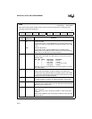
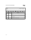
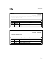
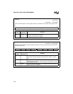
TH2, TL2
Address: TH2 S:CDH
TL2 S:CCH
Reset State: 0000 0000B
TH2, TL2 Timer Registers. These registers operate in cascade to form the 16-bit timer register in timer
2.
7 0
High/Low Byte of Timer 2 Register
Bit
Number
Bit
Mnemonic
Function
7:0 TH2.7:0
TL2.7:0
High byte of the timer 2 timer register.
Low byte of the timer 2 timer register.
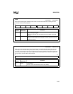
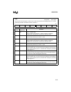
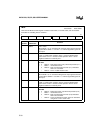
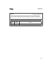
WCON
Address: S:A7H
Reset State: XXXX XX00B
Wait State Control Register. Use this register to enable the real time wait state input signal and/or the
wait state output clock.
7 0
———— ——RTWCERTWE
Bit
Number
Bit
Mnemonic
Function
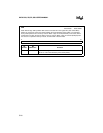
7:2 — Reserved:
The values read from these bits are indeterminate. Write “0” to these
bits.
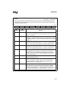
1 RTWCE Real time WAIT CLOCK enable. Write a ‘1’ to this bit to enable the WAIT
CLOCK on port 1.7 (WCLK). The square wave output signal is one-half
the oscillator frequency.
0 RTWE Real time WAIT# enable. Write a ‘1’ to this bit to enable real-time wait-
state input on port 1.6 (WAIT#).


