S3C8245/P8245/C8249/P8249 SERIAL I/O INTERFACE
16-3
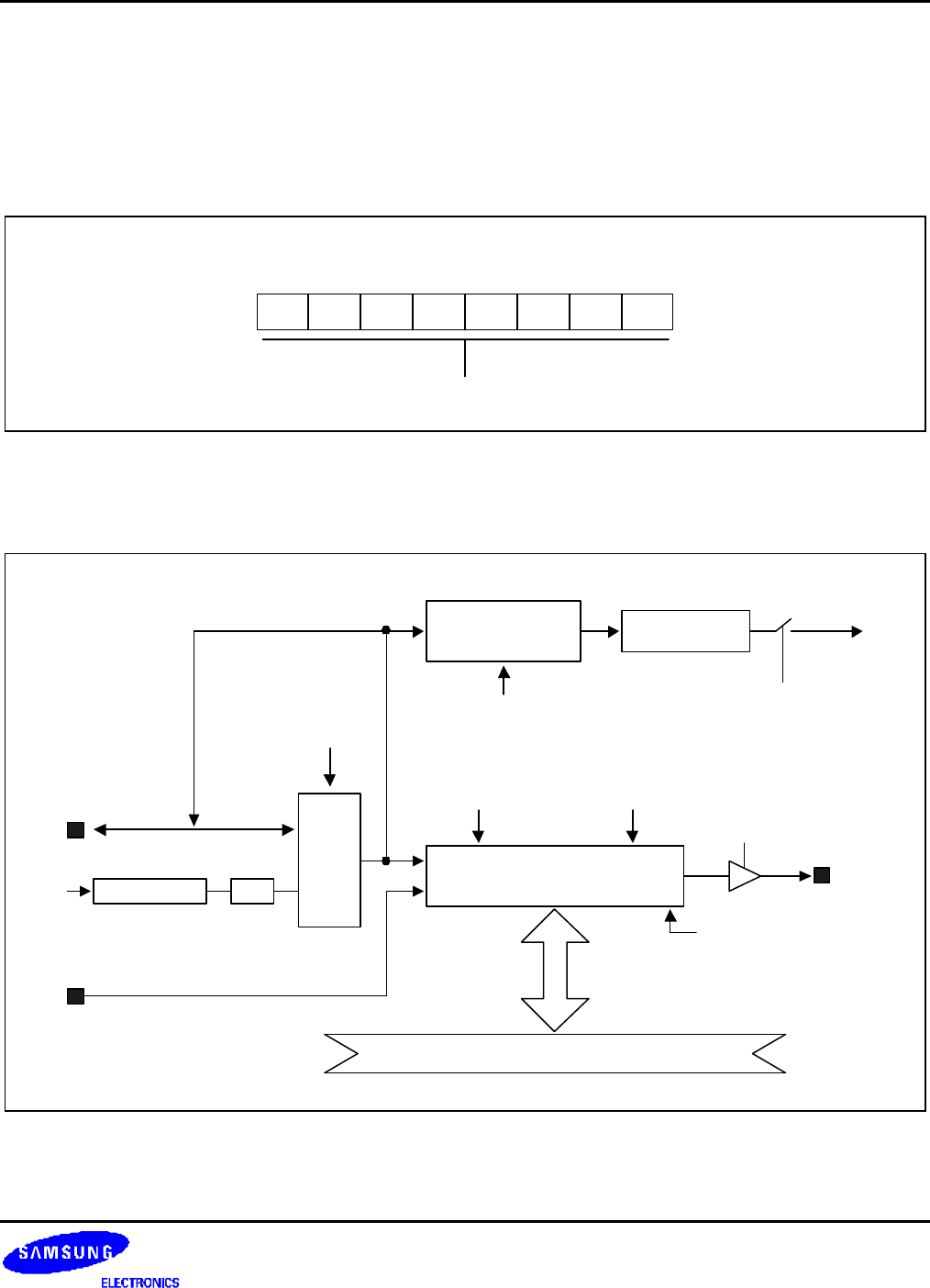
SIO PRE-SCALER REGISTER (SIOPS)
The control register for serial I/O interface module, SIOPS, is located at F2H in set 1, bank 0.
The value stored in the SIO pre-scale registers, SIOPS, lets you determine the SIO clock rate (baud rate) as follows:
Baud rate = Input clock (fxx/4)/(Pre-scaler value + 1), or SCK input clock, where the input clock is fxx/4
SIO Pre-scaler Register (SIOPS)
F2H, Set 1, Bank 0 R/W
.7 .6 .5 .4 .3 .2 .1 .0MSB LSB
Baud rate = (f
XX
/4)/(SIOPS + 1)
Figure 16-2. SIO Pre-scale Registers (SIOPS)
BLOCK DIAGRAM
SIO INT
Pending
3-Bit Counter
Clear
SIOCON.0
fxx /2
SIOPS (F2H, bank 0)
SCK
SIOCON.7
Prescaler Value = 1/(SIOPS +1)
SIOCON.1
(Interrupt Enable)
CLK
SI
SIOCON.3
Data Bus
SO
M
U
X
1/28-bit P.S.
IRQ4
8
8-Bit SIO Shift Buffer
(SIODATA, F1H, bank 0)
CLK
SIOCON.4
(Edge Select)
SIOCON.5
(Mode Select)
SIOCON.2
(Shift Enable)
SIOCON.6
(LSB/MSB First
Mode Select)
Figure 16-3. SIO Functional Block Diagram


