


Philips Semiconductors
User’s Manual - Preliminary -
P89LPC901/902/903
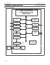
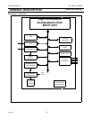
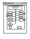
GENERAL DESCRIPTION
2003 Dec 8 15
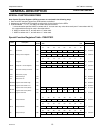
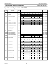
PIN DESCRIPTIONS - P89LPC903
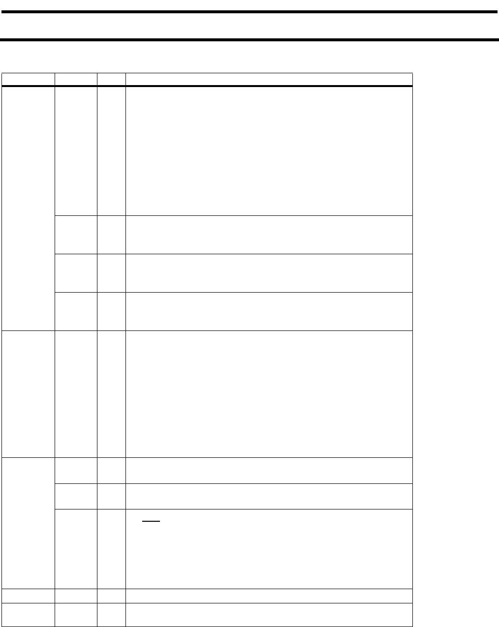
MNEMONIC PIN NO. TYPE NAME AND FUNCTION
P0.0 - P0.6 2,6,7 I/O Port 0: Port 0 is an I/O port with a user-configurable output types.
During reset Port 0 latches are configured in the input only
mode with the internal pullup disabled. The operation of port
0 pins as inputs and outputs depends upon the port
configuration selected. Each port pin is configured
independently. Refer to the section on I/O port
configuration and the DC Electrical Characteristics in the
Data Sheet for details.
The Keypad Interrupt feature operates with port 0 pins.
All pins have Schmitt triggered inputs.
Port 0 also provides various special functions as described below.
2I/OP0.2 Port 0 bit 2.
I CIN2A Comparator 2 positive input.
I KBI2 Keyboard Input 2.
7I/OP0.4 Port 0 bit 4.
I CIN1A Comparator 1 positive input.
I KBI4 Keyboard Input 4.
6 I/O P0.5 Port 0 bit 5.
I CMPREFComparator reference (negative) input.
I KBI5 Keyboard Input 5.
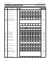
P1.0 - P1.5 3,4,5 Port 1: Port 1 is an I/O port with a user-configurable output types.
During reset Port 1 latches are configured in the input only
mode with the internal pull-up disabled. The operation of the
configurable port 1 pins as inputs and outputs depends
upon the port configuration selected. Each of the
configurable port pins are programmed independently.
Refer to the section on I/O port configuration and the DC
Electrical Characteristics in the Data Sheet for details. P1.5
is input only.
All pins have Schmitt triggered inputs.
Port 1 also provides various special functions as described below.
5I/OP1.0 Port 1 bit 0.
O TxD Serial port transmitter data.
3I/OP1.1 Port 1 bit 1.
I RxD Serial port receiver data.
4IP1.5 Port 1 bit 5. (Input only)
I RST
External Reset input during power-on or if selected via
UCFG1. When functioning as a reset input a low on this pin
resets the microcontroller, causing I/O ports and peripherals
to take on their default states, and the processor begins
execution at address 0. Also used during a power-on
sequence to force In-Circuit Programming mode.
V
SS
8IGround: 0V reference.
V
DD
1IPower Supply: This is the power supply voltage for normal operation as
well as Idle and Power down modes.