DIGITAL INPUT/OUTPUT CARD IOD-144 USER MANUAL
6-3
NOTE
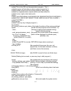
All data bits except D7 must be the same for the two control bytes
A, B, and C. If, for example, hex 80 is sent to Base Address+3, the Port 0 PPI
will be configured in mode 0 with ports A, B, and C as outputs.
But, at the same time, data bit D7 is also latched in a buffer controller for the
associated PPI chip. A high state disables the buffers and, thus, all associated buffers
will be put in the tristate mode; i.e., disabled.
c. When you wish to enable the output buffers, send a normal PPI mode command
with bit D7 low. For, example, if a control byte of hex 80 had been sent as
previously described, and it is now desired to open the three ports, you can
send a control byte of hex 00 to Base Address+3 to enable the port 0 buffers.
c. Those buffers will now remain enabled until another control byte with data
bit D7 high is sent to Base Address+3.
Those buffers will now remain enabled until another control byte with data bit D7 high
is sent to Base Address +3.


