DIGITAL INPUT/OUTPUT CARD IOD-144 USER MANUAL
6-2
NOTE:
Contact ACCES for directions if you wish to operate this
card in mode 1. This card cannot be operated in mode 2
The IOD-144 uses six 8255-5 PPIs to provide a total of 144 bits input/output capability.
The card is designed to use each of these PPIs in mode 0 wherein:
a. There are two 8-bit ports (A and B) and two 4-bit ports (C Hi and C Lo).
b. Any port can be configured as an input or an output.
c. Outputs are latched.
d. Inputs are not latched.
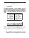
Each PPI contains a control register. This Write-only, 8-bit register is used to set the
mode and direction of the ports. At Power-Up or Reset, all I/O lines are set as inputs.
Each PPI should be configured during initialization by writing to the control registers even
if the ports are going to be used as inputs. Output buffers are automatically set by
hardware logic according to the control register. Control registers are located at base
addresses +3, +7, +B, +F, and +17. Bit assignments in each of these control registers are
as follows:
Bit Assignment Function
D0
D1
D2
D3
D4
D5,D6
D7
Port C Lo (C0-C3)
Port B
Mode Selection
Port C Hi (C4-C7)
Port A
Mode Selection
Mode Set Flag
1 = Input, 0 = Output
1 = Input, 0 = Output
1 = Mode 1, 0 = Mode 0
1 = Input, 0 = Output
1 = Input, 0 = Output
01 = Mode 1, 00 = Mode 0
1X = Mode 2
1 = Active
IOD-144 provides a means to enable/disable the tristate I/O buffers under program control.
If the BEN/TST jumper on the card is installed in the BEN position, the I/O buffers are
permanently enabled. However, if the jumper is placed in the TST position, enable/disable
of the buffers is possible under software control via the Control Register as follows:
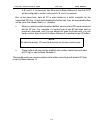
a. The card is initialized in the receive mode by the computer Reset command.
b. When bit D7 of the Control Register is set high, the direction of the three ports
of the associated PPI chip as well as the mode can be set. For example, a write
to Base Address+3 with data bit D7 high programs port direction of Port 1 ports


