Philips Semiconductors
User’s Manual - Preliminary -
P89LPC901/902/903
GENERAL DESCRIPTION
2003 Dec 8 24
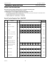
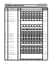
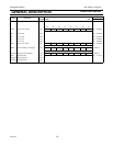
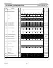
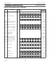
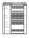
Notes:
* SFRs are bit addressable.
# SFRs are modified from or added to the 80C51 SFRs.
- Reserved bits, must be written with 0’s.
§ BRGR1 and BRGR0 must only be written if BRGEN in BRGCON SFR is ’0’. If any of them is written if BRGEN = 1, result is
unpredictable.
Unimplemented bits in SFRs (labeled ’-’ ) are X (unknown) at all times. Unless otherwise specified, ones should not be written to
these bits since they may be used for other purposes in future derivatives. The reset values shown for these bits are ’0’s
although they are unknown when read.
1. All ports are in input only (high impendance) state after power-up.
2. The RSTSRC register reflects the cause of the P89LPC901/902/903 reset. Upon a power-up reset, all reset source flags are
cleared except POF and BOF - the power-on reset value is xx110000.
3. After reset, the value is 111001x1, i.e., PRE2-PRE0 are all 1, WDRUN=1 and WDCLK=1. WDTOF bit is 1 after watchdog
reset and is 0 after power-on reset. Other resets will not affect WDTOF.
4. On power-on reset, the TRIM SFR is initialized with a factory preprogrammed value. Other resets will not cause initialization
of the TRIM register.
5. The only reset source that affects these SFRs is power-on reset.
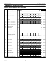
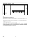
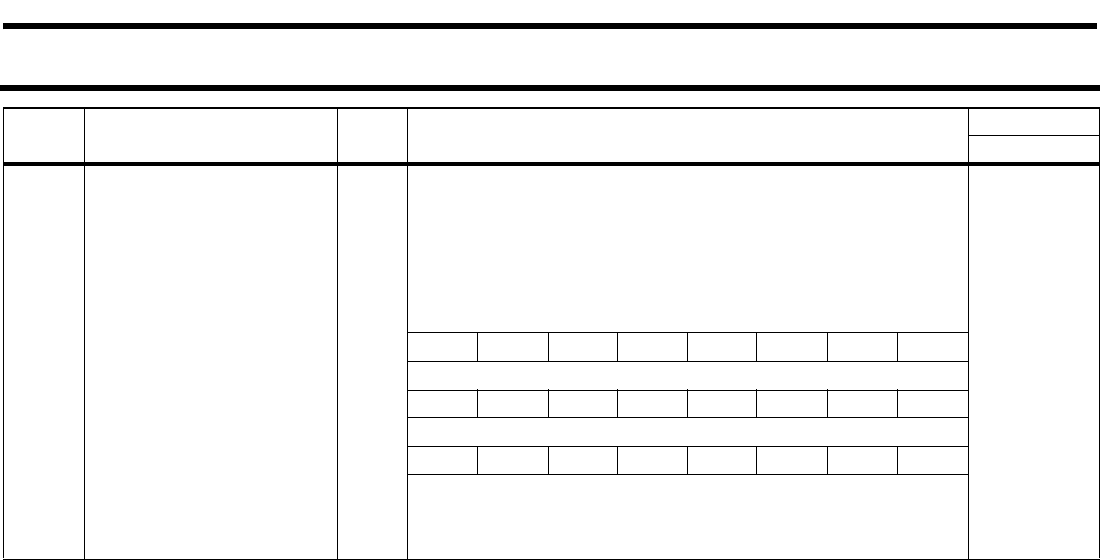
TH0 Timer 0 High 8CH 00H 00000000
TH1 Timer 1 High 8DH 00H 00000000
TL0 Timer 0 Low 8AH 00H 00000000
TL1 Timer 1 Low 8BH 00H 00000000
TMOD Timer 0 and 1 Mode 89H - - T1M1 T1M0 - - T0M1 T0M0 00H 00000000
TRIM# Internal Oscillator Trim Register 96H - - TRIM.5 TRIM.4 TRIM.3 TRIM.2 TRIM.1 TRIM.0 Notes 4,5
WDCON# Watchdog Control Register A7H PRE2 PRE1 PRE0 - - WDRUN WDTOF WDCLK Notes 3,5
WDL# Watchdog Load C1H FFH 11111111
WFEED1# Watchdog Feed 1 C2H
WFEED2# Watchdog Feed 2 C3H
Name Description
SFR
Address
Bit Functions and Addresses Reset Value
MSB
LSB
Hex Binary


